mobile background

Area Selective Atomic Layer Deposition (ASD Team)

Area-selective atomic layer deposition (AS-ALD)

Area-selective atomic layer deposition (AS-ALD) is a bottom-up fabrication process that employs surface chemistry to deposit thin-film material in a targeted area while maintaining large area uniformity, excellent conformality, and angstrom-level thickness control. Therefore, it can enable a reduction in the number of lithography and etch steps and in the use of hazardous reagents during the patterning process for electronic device fabrication, resulting in a decrease of edge placement errors as well as a drop in manufacturing costs.

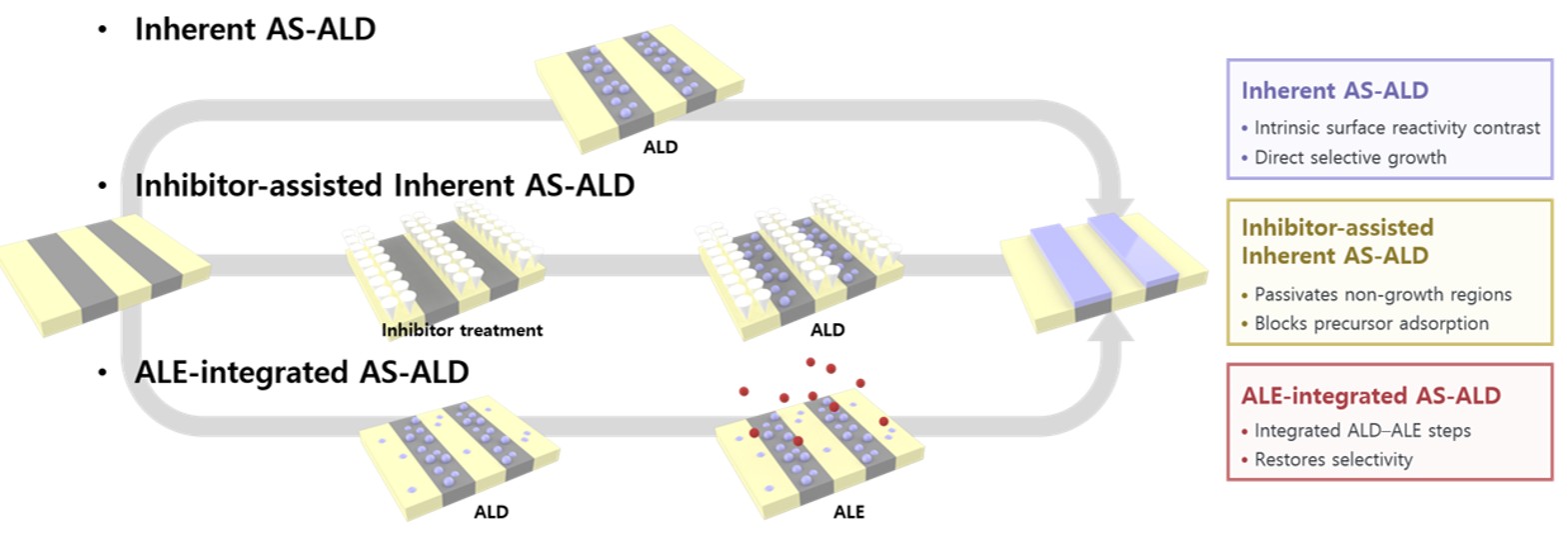
Both standard ALD and AS-ALD processes are strongly dependent on the ALD chemistry used. So, surface engineering is a key technique to enable to control of molecular adsorption. In AS-ALD, the chemical properties of a surface are controlled to activate or deactivate adsorption of the ALD precursors, so that patterns are formed through selective deposition across differently terminated domains. For instance, area-selective growth can be achieved through various strategies : inherent AS-ALD utilizing the intrinsic reactivity differences of substrates, inhibitor-assisted surface passivation to block precursor adsorption, and ALE-integrated AS-ALD that incorporates atomic layer etching steps to restore selectivity. Therefore, selective chemical deactivation of oxide surfaces has been a major challenge in the implementation of AS-ALD. By tuning this surface chemistry, we can facilitate the selective growth of materials in desired growth areas.


AS-ALD Application

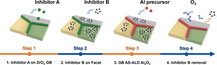
In ZrO₂/Al₂O₃/ZrO₂ capacitor stacks, AS-ALD can be used to selectively modify highly reactive sites such as grain-boundary regions. Selective Al₂O₃ passivation can suppress leakage pathways while maintaining the electrical advantages of the ZAZ structure.

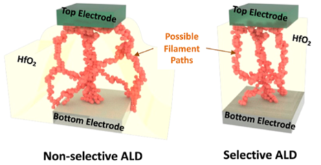
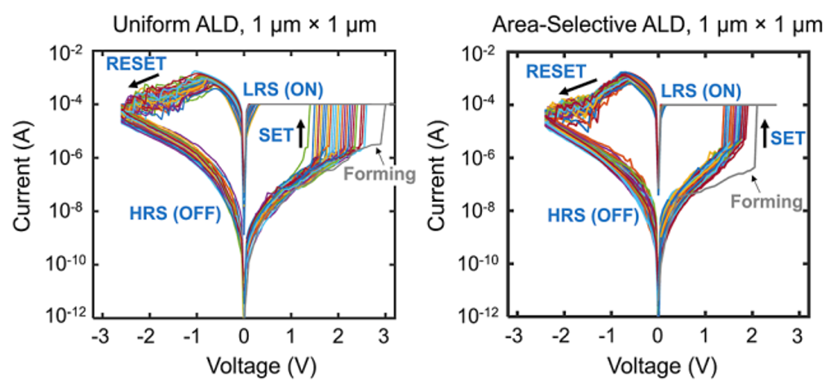
Using AS-ALD, the HfO2 dielectric active layer was selectively deposited on patterned Pt bottom electrodes while suppressing growth on the surrounding SiO2/Si regions, without requiring an additional photolithography step for HfO2 patterning. This area-confined HfO2 switching layer improves the structural precision of RRAM devices and reduces device variability by limiting the possible locations of conductive filament formation. As a result, AS-ALD-based RRAM devices showed a narrower SET voltage distribution and more stable resistance states compared with devices fabricated using nonselective HfO2 ALD.